nanoDTL Research

Research Interests

Nanoarchitectonics

    This is an emerging field of research that utilizes and develops nanotechnology to explore transformative computational devices, circuitries, and architectures. Although the dimensional scaling of conventional CMOS has been rather successful, the accompanying variability and manufacturing defects have also dramatically gone up. Their mitigations using traditional circuit-level techniques might in turn compromise the projected density advantages, especially with deeply-scaled devices. In collaboration with Prof. C. Andras Moritz at UMass, nanoDTL has been developing an innovative fabric architecture based on semiconductor nanowires and targeting data-paths with built-in fault resilience modules. This fabric architecture, known as Nanoscale Application Specific IC (NASIC), is constructed using tile-based 2D semiconductor nanowire grids, which has been theoretically projected to deliver an overall performance-power-density advantage over its CMOS counterpart.

    nanoDTL is responsible to experimentally develop the essential 2D orthogonal nanowire fabric and intrinsic switching devices therein. For the nanowire fabric synthesis, we have been focusing on an original hybrid top-down and bottom-up approach that simultaneously offers an intrinsic and VLSI-ready control over key parameters including the number of nanowires, inter-nanowire pitch, and nanowire diameter. For the switching cross-nanowire field-effect transistor (xnwFET) development, we have been devising a novel structure with selectively enhanced gate-to-channel coupling through the inherently tiny contact cross point. Our bigger research goal here is to identify feasible NASIC manufacturing pathway and demonstrate NASIC prototypes.

Nanotheranostics

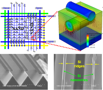
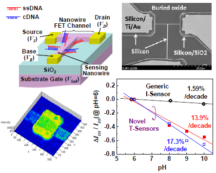
    This is a rapidly growing, interdisciplinary field of research field spanning across nanoscience, medical therapy, and disease diagnostics. The advances in understanding and manipulation of nanoscale scientific phenomena have indeed offered unprecedented opportunities and capabilities to address timely medical and biological problems. Our grand research mission is to develop very low-cost and high impact disease diagnostic platforms for deployment at the point-of-care (POC). The criteria on the signal transduction device technology include superior sensitivity, multiplex and simple operations, response timeliness, compactness, reusability, simple fabrication, and electronic interfaces. As a contending POC diagnostic platform component technology, semiconductor nanowire FET sensors permit visual-label-free and real-time electronic detections of numerous charged biomarkers with high sensitivity and great selectivity. These detection sensitivity and selectivity need, however, to be further improved to meet the POC diagnostic requirements.

    While many pioneering research efforts have been focusing on either the development of nanowire material and fabrication, or detection of unconventional biomolecules, nanoDTL exploits the fundamental scientific principles and engineering measures to maximize the detection sensitivity and selectivity. Selected specific research directions include: (i) exploring the fundamental relationships between voltage biasing, analyte type, and counter ion strength, (ii) formulation of inventive voltage biasing schemes, and (iii) development of transformative nanowire FET biosensor structures. To ensure our scientific research accomplishments can be translated into practical medical devices, we have maintained experimental collaborations with colleagues at Molecular and Medical Pharmacology, Center for Small Bowel Diseases, and others in our top-ranking School of Medicine at UCLA.

Nanoelectronics

    Within this general yet broad research field, nanoDTL has been focusing on two major aspects: terahertz power transistor and device variability.

    For microwave power amplifier applications, we are developing a transistor concept that promises the delivery of concurrent frequency and power gains in excess of 1 THz. It embraces the respective structural advantages of high electron mobility transistor (HEMT) and heterojunction bipolar transistor (HBT) as well as a low bandgap ultrahigh mobility compound semiconductor channel material. It also has a unique structure to improve the device linearity with minimal modification to its fabrication.

    As feature sizes shrink, device variability is becoming a significant obstacle to continuous CMOS scaling besides power consumption. Sources of variation include line edge roughness (LER) and/or line width roughness, random dopant fluctuation, oxide thickness fluctuation, work function variation, and others. We have been studying the impacts of these variations on device performance.


UCLA Infrastructures